Description
Chip on Board COB
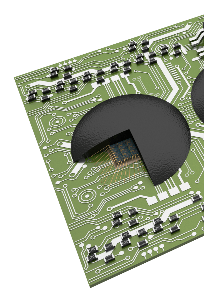
Chip on board (COB) packages are a type of electronic packaging technology that involves mounting a semiconductor chip directly onto a printed circuit board (PCB) or substrate. COB packaging is a way to integrate the chip and the substrate into a single unit, rather than using a traditional package with leads or pads.
There are several steps involved in making a COB package:
- The first step is to prepare the substrate by cleaning it and applying a thin layer of conductive material, such as copper, to the surface.
- The semiconductor chip is then placed onto the substrate and aligned with the conductive traces on the substrate.
- The chip is then bonded to the substrate using a conductive adhesive, such as silver die attach epoxy, silicone, or acrylate.
- The bond wires are then attached to the chip and the substrate using a wire bonding process. This process involves using a machine to place very thin wires between the chip and the substrate, creating electrical connections between the two.
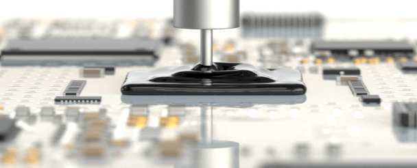
- Once the bond wires are in place, the COB package is sealed with a protective material, such as an epoxy molding compound or a liquid encapsulant, to protect the chip and the bond wires from damage.
COB packages offer several advantages over traditional packaging methods, including a smaller overall size, improved performance, and a lower cost of production. They are commonly used in a wide range of electronic devices, including smartphones, tablets, and other portable electronics.
Encapsulation

Chip on board encapsulants feature:
- Protection of wire bonded dies on substrates against mechanical and chemical impacts
- Provides localized protection of sensitive components and as such allows the electronic packages to pass reliability targets
- To minimize corrosion of wire bonds and silicon die (protection against moisture)
- To act as dielectric – isolate wires from each other
Dam & Fill
Dam and fill encapsulation is a method of packaging semiconductor chips in which a layer of material, such as epoxy, is applied around the chip and then “filled” with another material, such as a fill encapsulant. It forms a”dam” around the edges of the chip, and then filling it, protecting it from mechanical damage and other environmental factors.
The dam and fill process typically involves the following steps:
- The semiconductor chip is placed onto a substrate or PCB.
- A layer of protective material, such as epoxy, is applied around the chip.
- The filled material is then applied over the die and around the edges of the chip.
- Both materials are then cured, or hardened, using heat or UV light.
Dam and fill encapsulation is commonly used to protect semiconductor chips in applications where the chips may be subjected to mechanical stress, such as in automotive or aerospace systems. It provides a high level of protection for the chip, helping to ensure reliable operation in harsh environments.

Dam and fill typical dispense patterns
Additional information:
- A dam is a perimeter of fluid dispensed around a die mounted on a substrate that limits the flow out of the fill material
- Dam height should be at least 200µm higher than the highest wire bond
- A dam is the high thixotropic version of the lower viscous encapsulant, creating a wall around the device.
- The cavity fill is a low viscous fluid to cover or encapsulate the die to provide protection and extend the life time of the wire bonded die
- The fill encapsulant is designed to have high flow characteristics to allow easy penetration in and around ultra fine pitch wires.

Pls contact us for more information : Email – [email protected]


